PsyLink is experimental hardware for reading muscle signals and using them to e.g. control the computer, recognize gestures, play video games, or simulate a keyboard. PsyLink is open source, sEMG-based, neural-network-powered, and can be obtained here.
This blog details the steps of building it and shows recent developments. Subscribe to new posts with any RSS reader, and join the community on the Matrix chatroom.
- All posts on one page
-
2025-05-01: PsyLink Talk
-
2024-08-16: Mass Production #2
-
2024-08-01: Android: First Step
-
2024-07-25: Rev2 Firmware
-
2024-07-24: Prototype Fund
-
2023-08-25: Data Sheets
-
2023-05-31: Prototype 10
-
2023-03-22: Enhanced Signal by >1000%
-
2023-03-06: Sample Signals
-
2023-02-05: 2022 Retrospective
-
2022-02-24: Added Bills of Materials
-
2022-02-23: 3M Red Dot electrodes
-
2022-02-22: Microchip 6N11-100
-
2022-02-16: Next Steps & Resources
-
2022-02-15: Mass production
-
2022-01-19: Prototype 9 + Matrix Chatroom
-
2022-01-18: HackChat & Hackaday Article
-
2021-12-19: Prototype 8 Demo Video
-
2021-12-18: Prototype 8
-
2021-12-16: INA155 Instrumentation …
-
2021-12-15: Power Module 4
-
2021-11-30: Batch Update
-
2021-07-17: Neurofeedback: Training in …
-
2021-07-06: New Frontpage + Logo
-
2021-06-24: Cyber Wristband of Telepathy …
-
2021-06-21: Running on AAA battery
-
2021-06-16: Power Module 3
-
2021-06-10: Believe The Datasheet
-
2021-06-04: Back to the Roots
-
2021-05-31: Website is Ready
-
2021-05-29: Dedicated Website
-
2021-05-17: Gyroscope + Accelerometer
-
2021-05-14: Wireless Prototype
-
2021-05-09: Power Supply Module
-
2021-05-07: New Name
-
2021-05-06: Finished new UI
-
2021-05-04: Higher Bandwidth, new UI
-
2021-04-30: PCB Time
-
2021-04-29: Soldering the Processing Units
-
2021-04-28: Going Wireless
-
2021-04-24: First Amplifier Circuit
-
2021-04-19: Amplifiers
-
2021-04-15: Multiplexers
-
2021-04-14: Data Cleaning
-
2021-04-13: Cyber Gauntlet +1
-
2021-04-11: Adding some AI
-
2021-04-09: F-Zero
-
2021-04-08: Baby Steps
-
2021-04-03: The Idea
Running on AAA battery
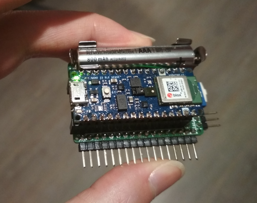
└2021-06-21, by RomanWow, it feels like ages since I started working on making PsyLink run on a rechargeable AAA battery. It sounds so simple and straight-forward, but it wasn't :). This ate 2.5 weeks of my time, but finally I succeeded!
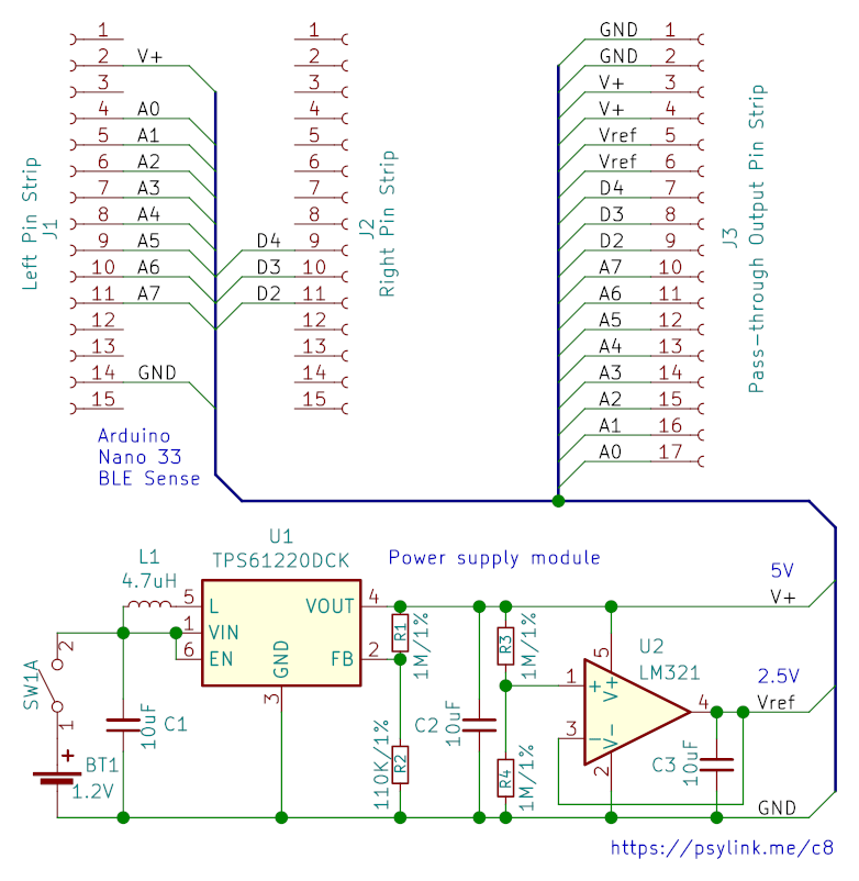
Coming from software engineering, the iteration time of hardware prototypes is horribly slow. There was a lot of waiting for package deliveries, a lot of time assembling, and a lot of wrestling with leaky abstractions. For example, it wasn't enough to just connect the 1.2V->5V boost converter like on the circuit diagram, but I had to take special care of the distances between the parts, and the widths of the copper tracks connecting them.
Another problem you never face in software engineering is that the package with electronics parts was stolen, and when the new PCB of arrived, I had to work with the few remaining (suboptimal) parts that I had.
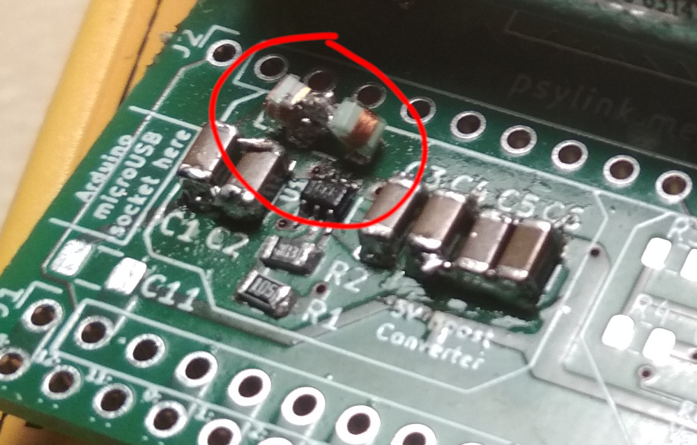
What almost drove me insane was that I had only one fresh TPS61220 chip left. That's the 5V boost converter at position U1 (in the bottom of the red circle on the photo below), which is so small that I don't really have the tools to solder it on properly. I kept accidentally connecting the pins of the chip with solder. I gave up and started asking around friends for whether they could solder it on for me, when I remembered this soldering tip someone gave me: If you don't have soldering flux (which I didn't have), just use ✨margarine✨ instead ;D. It sounds very wrong, but it actually made a huge difference, and only thanks to the power of margarine I was able to keep the solder exactly where I needed it to be. "If it's stupid and it works, it's not stupid."
Then - for whatever reason - the voltage was going up to 1.5V instead of 5V, just like with the previous PCB layout. I thought I fixed that problem by optimizing the layout around the TPS61220 chip, but apparently that wasn't enough. I figured the 4.7µH inductance at L1 wasn't big enough, so I squeezed in a second coil:
(It looks like two tardigrades playing ball :) I wish I made a better picture before I disassembled it again)
This alone didn't help, but when I manually held an additional 10µH inductance in parallel to L1 for 1 second while the device was running, it surprisingly kickstarted and reached 5V!... until I drained some current, which made the voltage collapse back to 1.5V immediately. Curious behavior. :D
Then I tried soldering on the big 10µH coil directly onto the SMD pads, and the voltage reached 5V and stayed at 5V =)
No idea why the big 10µH coil worked while the two smaller coils totaling 9.4µH didn't work... I doubt that the 0.6µH difference in total inductance turned the tide, probably there's some factor I'm not aware of. I actually had ordered a 10µH SMD inductance coil in anticipation of this, but well, it got stolen... My only consolation is the face of the package thieves when they open the package, they realize that it's just a couple of tiny SMD parts, and they wonder WTF this shit is even good for.
P.S.: I found out that the reason why the coils didn't work was that they were not rated for the >200mA that's passing through them. Once I got a 4.7µH coil rated for 280mA, everything was fine.
More pictures:
The lack of parts forced me to adjust the resistance/inductance/capacitance values of :
Thankfully I had planned for way too many capacitors on the PCB, just for some extra VROOOM, so the fact that I only had 10µF capacitors instead of the planned 100µF didn't matter too much.
I also changed the 1MΩ resistors in the reference voltage generator to 110kΩ because I read that smaller resistances in a voltage divider make the output voltage more stable, at the cost of more power use, but I think we can sacrifice some power for signal accuracy. No idea whether it's actually going to help though. I chose 110kΩ instead of the more common 100kΩ and 220kΩ because the boost converter already requires a 110kΩ resistor, and that way this prototype requires fewer different parts. But the exact values don't matter, as long as both resistances are identical.
Tomorrow I'll start working on the electrodes and wristband. :)
Power Module 3
└2021-06-16, by RomanSince Power Module 2 has the wrong PCB layout for the step-up converter, I built to fix this issue.
It was still a worthwhile learning experience to build Power Module 2, resulting in the following changes:
- Instead of stacking the Arduino and the Battery on top of each other (one on the front side of the board, one on the back), they're now side by side, to make the board flatter and fit better on the forearm.
- Added more capacitors all over the place
- Added various jumpers:
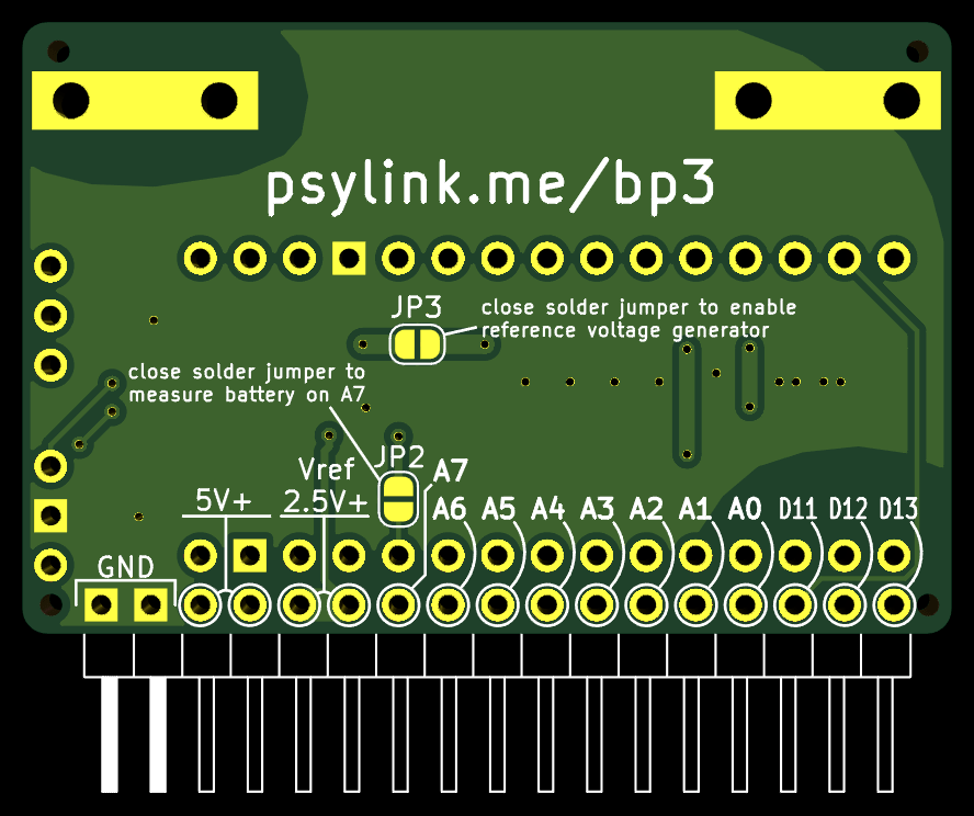
- A solder jumper to enable/disable the reference voltage generator, in case I come up with a setup where I won't actually need it
- A solder jumper to sacrifice one electrode and use its analog input pin to measure the battery charge instead.
- Three configuration pins, connectable via jumpers, to change software settings on the fly and toggle between up to 4 different modes. Or you can use them to plug in an extra module.
- Hopefully fixed the layout for the step-up converter
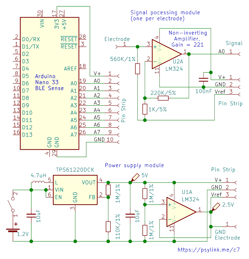
Here's the circuit:
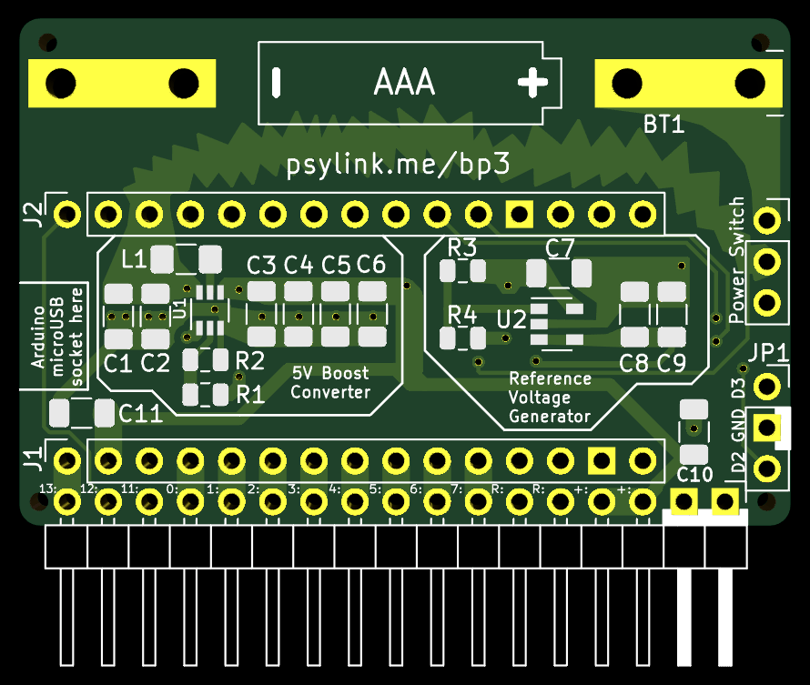
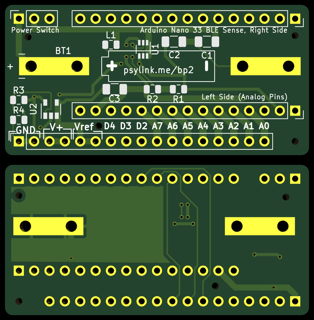
And the new PCB:
If you're wondering why the sparky, fancy looking power line goes all the way from the power switch on the right through digital pin D10 and into L1 on the left side... Indeed that looks pretty awkward, but L1 is the noisiest component, and I wanted to keep it as far as possible from the analog pins at the bottom, without sacrificing the effectiveness of the boost converter layout. Given the size & time constraints, I didn't find a better solution.
What time constraints, you ask? Well, actually I made a different PCB layout first. Polished every detail, and when it was perfect (according to my crude appraisal), I ordered it. Was already excited about the delivery, started putting the board on the website, and so on. But at some point I noticed that something was wrong... The Arduino pins were inverted. Theoretically, everything would still work, but the Arduino would have to be plugged in from the back side, which is something I wanted to avoid to keep the board laying nice and flat on the forearm...
Thankfully the manufacturing process hasn't started yet, and I could update the board for free. So I started redesigning half of the board and finished just in time for the production to start :D
Let's hope it works this time.
Believe The Datasheet
└2021-06-10, by RomanToday the order of Power Module 2 arrived!
And with relief I saw that the battery clips fit nicely onto the board, as does the Arduino (with pin strips), and all the other components. Just that simple thing already felt like an accomplishment at my level of expertise with PCB design ;)
After some dreadful time trying to solder on the tiny 1x2mm-sized chip at U1 (I need a microscope for this shit), I had the SMD parts assembled and the circuit was ready for a test drive:
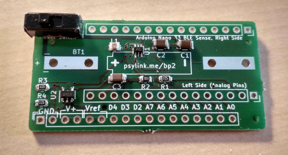
But something was weird. The output voltage was a meager 1.5V, not the expected 5V, even though everything was connected properly. After hours of debugging I flipped over the table and just soldered a fresh board, this time without the Vref-generating OpAmp (U2+R3+R4+C3). But no luck, still just 1.5V. This was lower than the minimal output voltage of the voltage booster, so the chip didn't even finish it's start-up phase. How could that be, if there's not even any load on the output voltage?
I desperately tried several different things. One was doubling the inductance at L1 from 4.7µH to 9.4µH by using two SMD inductances in series:
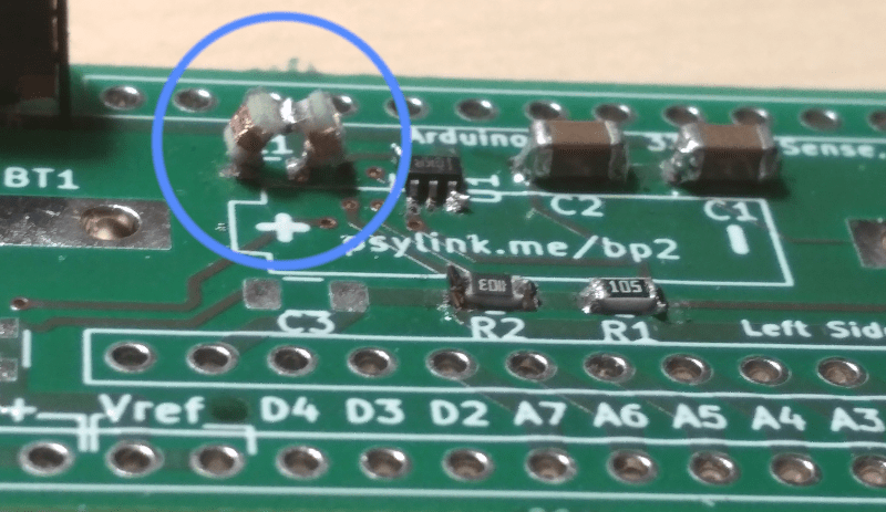
Unfortunately I think I broke the coils while constructing this, since they didn't let any current go through. But I found a regular, big inductance coil with 10µH, manually held its pins down onto the SMD pads, and indeed, the voltage jumped up to 5V!
So I soldered it... onto... the SMD pads.

(Probably you can reconstruct my entire room from all the reflections in this image, along with a biometric picture of my face and at least 3 of my fingerprints...)
But once I connected the OpAmp, the voltage went back down to 2.5V, and with the Arduino connected, it went down further to 2.4V. Adding a second coil in series for a total of 20µH didn't compensate for this, but made it even worse, bringing it all the way down to 1.5V.
Well, clearly whatever is wrong with this construction has something to do with the inductance, and it's not purely the amount of inductance... Which brings us to the title of this post:
The mistake (probably)
Of course the data sheet of the voltage booster CLEARLY STATED that the inductance coil needs to be AS CLOSE AS PHYSICALLY POSSIBLE to the chip. The capacitors C1 and C2 too, by the way. And I even read that. But I thought, what could possibly go wrong if I move it ~1cm away to make some space for the battery? Nothing, right? Well, awesome, I guess it's time for another revision :)
At least the 2.4V were enough to power the Arduino, although it was visibly struggling. I could establish a Bluetooth connection and collect some signals, but the Bluetooth packets were coming in extremely slowly (though still faster than mobile internet in 80% of Germany.)
Pictures
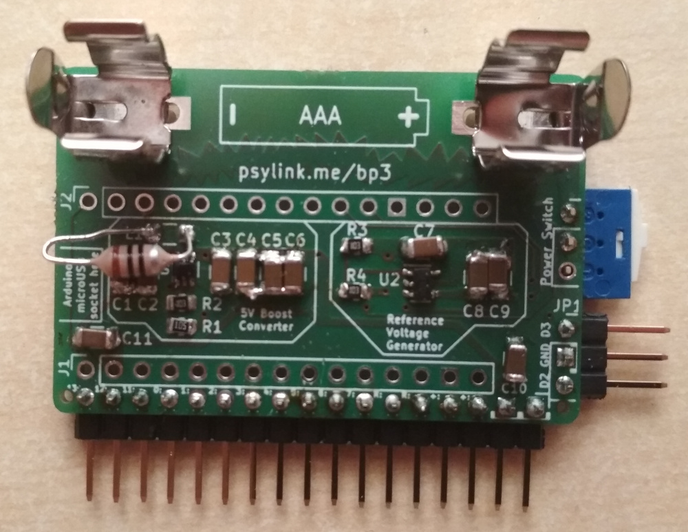
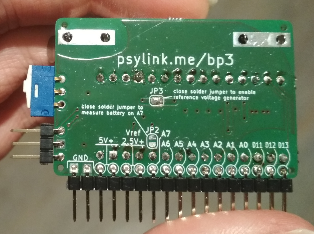
Front:
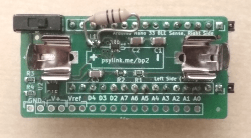
Somehow the oversized inductance coil adds a nice vibe to it.
Front, with battery:
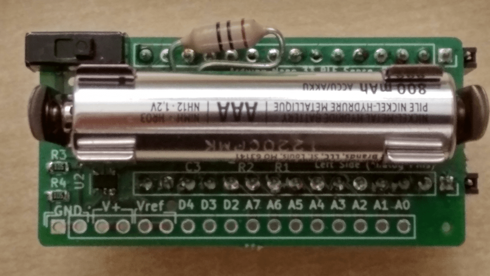
Back, with attached Arduino:
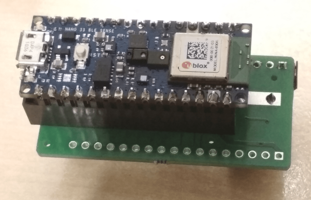
This picture shows a pin strip socket that will be gone in the final version, where the Arduino will be soldered onto the board, reducing the height from 3cm to 2cm.
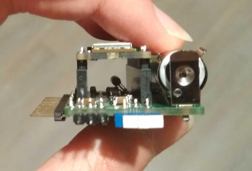
Side, with Arduino and battery:

(Yes, the pin strip socket is too long by one pin ;))
Back to the Roots
└2021-06-04, by RomanWhile uploading the old videos to the new PeerTube channel, I viewed the first video once again, which shows a pretty good signal from just two pieces of aluminum foil taped to the skin. And I wondered, why do I even bother with such a complicated set-up like in Prototype 4? It was really annoying to assemble, and the device is clunky and fragile.
Let's go back to the roots and build something more simple. Plenty of reasons:
- Having 8 small, distributed signal processing PCBs sounds nice at first, but it creates more points of failure. With Prototype 4, I had multiple instances where a connecting wire broke off, so this time I'd rather have everything on one PCB.
- What happened to the idea of processing the signal as little as possible and leaving the job to the neural network? Circuit 6 (whole device) amplifies certain information but hides other, like the DC voltage offset between electrodes.
- The electrode map of Prototype 4 provides me with signals (like "arm
turns left/right") which are redundant since I added support for the
inertial measurement unit (IMU).
- The signal from the IMU is actually way more reliable than what I'm getting from the electrodes, so why not ditch them completely? Well, there are some parts of the arm that move separately from the Arduino, mainly the fingers. So let's focus on these.
- My main issue with the early prototypes was the poor signal-to-noise ratio, but that was mainly due to the power line. This should be gone with a battery-powered device.
Circuit 7
The Circuit 7 (whole device) shows a simplification of the signal processing module to a simple non-inverting amplifier per electrode with a gain of 221x. There's also a 560KΩ bias resistor towards Vref so the voltage we measure isn't too far off the center. In Circuit 6 (whole device) I had used 1MΩ, but here it produced mysterious oscillations, and going down to 560KΩ mysteriously fixed it.
This circuit also features a rechargeable 1.2V AAA battery with a TPS61220 step-up converter boosting the voltage to 5V, because I don't hate nature, and I burned through enough CR2032 coin cells. Coin cells also aren't exactly optimized for currents of 20mA, and thus get drained too quickly.
I measured a signal while pressing down a finger onto the table with two electrodes along the Flexor Digitorum Superficialis. Blue is electrode 1, red is electrode 2, and green is an amplified difference:

Circuit 8
But let's cut even more out of this circuit. Here's one that is designed to be a shield to the Arduino Nano 33 BLE Sense, containing just the power supply, and an array of pass-through pins:
The signal that I'm getting is weaker, but certainly usable: (again, I measured a signal while pressing down a finger onto the table with two electrodes along the Flexor Digitorum Superficialis. Blue is electrode 1, red is electrode 2, and green is an amplified difference)

PCB
I also built a PCB that implements this power supply/pass-through shield, and I figured, even if the device ends up not very useful, I'll still be able to use this for experiments later on, thanks to the pass-through pins.
I just hope that the PCB/circuit will work at all. I still haven't figured out how to simulate it, and I don't really know the best practices for PCB design. The PCB footprint for the AAA battery clips (Keystone 82) is my first custom-made PCB footprint too. Hope it all works out.
Next Prototype
It will be a relatively small forearm band with 8 electrodes (+ 1 ground electrode), which I plan to place around the Flexor Digitorum Superficialis for detecting what individual fingers are doing. The information from the gyroscope + accelerometer should cover the rest.
Website is Ready
└2021-05-31, by RomanThe website is more fleshed out now, with a nice black/green design, neurons in the background, and a logo that is based on the logo of the fictional TriOptimum Corporation from the System Shock game series.
Videos are now hosted on a PeerTube Channel, allowing me to upload higher quality videos in the future while keeping the git repository of the website small.
I also catalogued individual components (circuit schematics, circuit boards, textiles, software) that resulted from this project so far, and documented how they all fit together in the prototype overview. Each component has an individual ID now, that I can easily write, print or sew on the hardware so I don't mix everything up. For example, prototype 4 has the ID "p4" and can be reached directly via https://psylink.me/p4, while the signal processing board of p4 has the ID "b1" and can be reached via https://psylink.me/b1.
Here's a screenshot, for a future time when the design has changed:
