PsyLink is experimental hardware for reading muscle signals and using them to e.g. control the computer, recognize gestures, play video games, or simulate a keyboard. PsyLink is open source, sEMG-based, neural-network-powered, and can be obtained here.
This blog details the steps of building it and shows recent developments. Subscribe to new posts with any RSS reader, and join the community on the Matrix chatroom.
- All posts on one page
-
2025-05-01: PsyLink Talk
-
2024-08-16: Mass Production #2
-
2024-08-01: Android: First Step
-
2024-07-25: Rev2 Firmware
-
2024-07-24: Prototype Fund
-
2023-08-25: Data Sheets
-
2023-05-31: Prototype 10
-
2023-03-22: Enhanced Signal by >1000%
-
2023-03-06: Sample Signals
-
2023-02-05: 2022 Retrospective
-
2022-02-24: Added Bills of Materials
-
2022-02-23: 3M Red Dot electrodes
-
2022-02-22: Microchip 6N11-100
-
2022-02-16: Next Steps & Resources
-
2022-02-15: Mass production
-
2022-01-19: Prototype 9 + Matrix Chatroom
-
2022-01-18: HackChat & Hackaday Article
-
2021-12-19: Prototype 8 Demo Video
-
2021-12-18: Prototype 8
-
2021-12-16: INA155 Instrumentation …
-
2021-12-15: Power Module 4
-
2021-11-30: Batch Update
-
2021-07-17: Neurofeedback: Training in …
-
2021-07-06: New Frontpage + Logo
-
2021-06-24: Cyber Wristband of Telepathy …
-
2021-06-21: Running on AAA battery
-
2021-06-16: Power Module 3
-
2021-06-10: Believe The Datasheet
-
2021-06-04: Back to the Roots
-
2021-05-31: Website is Ready
-
2021-05-29: Dedicated Website
-
2021-05-17: Gyroscope + Accelerometer
-
2021-05-14: Wireless Prototype
-
2021-05-09: Power Supply Module
-
2021-05-07: New Name
-
2021-05-06: Finished new UI
-
2021-05-04: Higher Bandwidth, new UI
-
2021-04-30: PCB Time
-
2021-04-29: Soldering the Processing Units
-
2021-04-28: Going Wireless
-
2021-04-24: First Amplifier Circuit
-
2021-04-19: Amplifiers
-
2021-04-15: Multiplexers
-
2021-04-14: Data Cleaning
-
2021-04-13: Cyber Gauntlet +1
-
2021-04-11: Adding some AI
-
2021-04-09: F-Zero
-
2021-04-08: Baby Steps
-
2021-04-03: The Idea
Power Module 4
└2021-12-15, by RomanPrototype 8 needs a matching power module. I can't continue to awkwardly stuff the rubber band between the velcro and the PCB of like this:

We need a PCB with proper rubber band holes and screw mounting points, so it can be worn along the radius bone with about 2x beside it.
Unfortunately the large dimensions of the Arduino and the battery make it a little difficult. There's several options to do this, but none of them are perfect:
- Place Arduino and battery beside each other like in
and either...
- make the board ~15mm longer to fit the holes.
- Downside: The rubber band holes would be wider apart than on the
- make the board ~12mm wider to fit the holes.
- Downside: It would be too wide to comfortably fit on the radius bone
- Downside of both options: it might feel unbalanced when worn on the side of the arm, because the heavy battery moves the center of mass off to the side
- make the board ~15mm longer to fit the holes.
- Place Arduino and battery on top of each other, with pin sockets for the arduino that are taller than the battery, then make the board the size of to fit the holes
- Downside: It might be hard to acquire pin sockets that tall
- Downside: Little space left for the holes and the remaining components, but might work
- Place Arduino and battery in a line next to each other and make the board 20mm longer and 8mm wider than to fit the holes.
- Downside: The rubber bands are relatively close to the center, reducing the force with which the far ends of the board are pressed onto the skin
- Downside: The large dimensions might make it too bulky
- Remove the Arduino and solder the NINA-B306 bluetooth module of the Arduino onto the board directly, along with all the peripherals I need
- Downside: Unnecessary complexity
- Downside: More difficult soldering
- Instead of adding any holes, just stack the board on top of a and use its screws and rubber band holes for physical support. (Thanks to PerlinWarp for that idea!)
- Downside: Would require a redesign of
- Downside: The height of the prototype might make it feel unbalanced
- Downside: The board would have be either wider or longer than the due to the dimensions of the Arduino and battery. As a result, it would stick out to the sides, unless I enlarge the electrode board as well.
In the end I chose option 3 for simplicity reasons, and because the downsides seemed the most acceptable. This also gives me a lot of space on the PCB which is currently not needed, but may be used for analog multiplexing later on, to allow supporting more than 8 electrodes.
I am quite tempted by option 2 though, it would make for a really compact board. Maybe I give it a try later (if I ever find a source for 1x15 pin sockets that are 14mm+ tall and 2.54mm spaced apart.)
Here is the resulting board. As you see, I also added a screw mounting hole in the center, which should point right at the bone, which perhaps makes for a great ground electrode. Any of the screws can be used as ground electrodes though, simply by closing their respective solder jumper. I will try out various combinations to see which one is best.
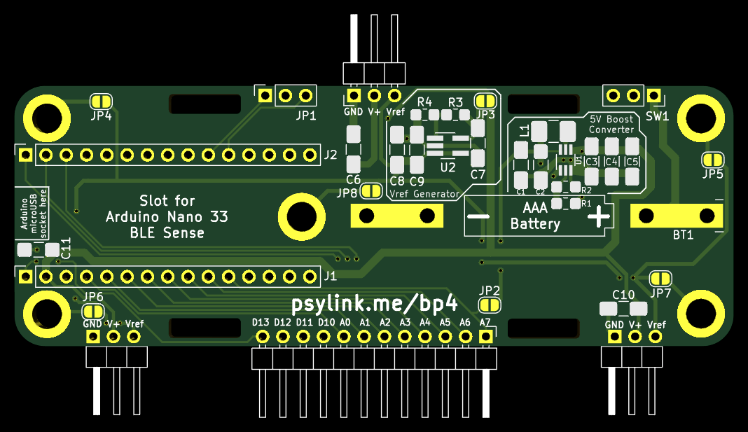
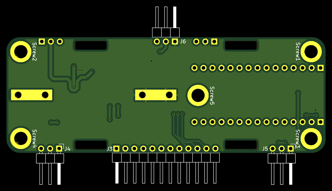
The matching circuit:

I ordered the production of this board already, and I'm excited to see if it will work out like I imagine. :)
Fun story on the side: I ordered the boards on Aisler, and they let you change the PCB design for free until it hits production. This time, I had a couple of hours left, which I used to make a couple of adjustments here and there, until I was happy and went to sleep. After 3 hours I woke up, with racing thoughts, and I couldn't really fall asleep again (which happens very rarely). After laying awake for 2 hours, it occurred to me that I should run the automatic PCB layout check of KiCad once again to test my board for obvious mistakes. Of course I had run the check before submitting my order, and several times after doing my various modifications. But as it turned out, I had indeed forgotten to run it on the final version, and there were multiple errors too! Several unconnected nodes and some copper tracks that were too close to each other. Luckily I caught this just a couple minutes before my time for free modification ran out, and fixed it just in time. Thanks insomnia.
Batch Update
└2021-11-30, by RomanI haven't been posting recently because I've been focusing on other areas of my life, but there has still been progress with PsyLink:
Prototype 6 improvements
I redesigned to be more easily hand-solderable by enlarging the solder pads and adding thermal clearances to some of the filled copper areas. (The copper tracks to several pads were so wide that the heat of the solder iron was dissipating too fast into the copper, and the pads were not heating up properly). The result is Power Module 3.1.
Prototype 7
PerlinWarp reached out to me, and after some fruitful conversations, I build a Prototype 7 for him for research purposes. It's a hybrid of Prototype 4 and Prototype 6 which combines the advanced with a cluster of Electrode Module 1 attached to Sleeve 3.
The assembly of the Prototype 7 took a full 20 hours of mindless labor, so I had a LOT of time to think about improvements to the design that would make it easier to assemble:
- Instead of having small boards for differential amplifiers that have to be tediously connected with three fragile wires, bulk four of them up in a single board.
- Instead of having a piece of custom-tailored fabric with precisely placed electrodes, use electrodes made of metal screw-like parts that fit right on to the PCB. The PCBs are held together with a rubber band that presses the electrodes tightly to the skin.
- Made more easily hand-solderable (described above)
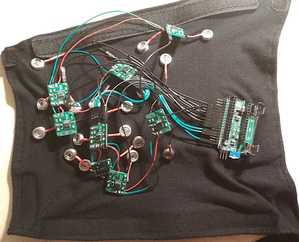
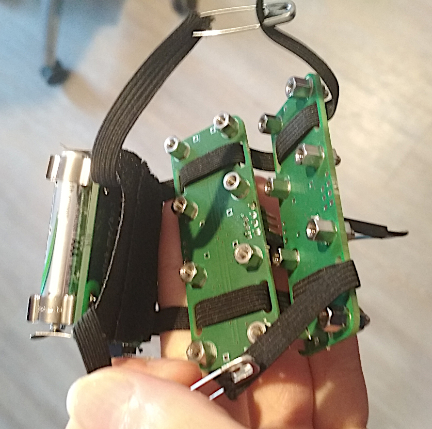
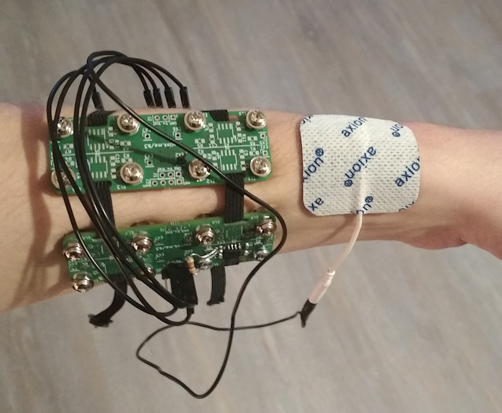
Prototype 8 (WIP)
The 8th prototype implements those changes, resulting in a device purely made of PCBs connected by rubber bands and wires. These PCBs rest on the skin on legs of metal, which double as the electrodes.
As of now, only the differential amplifiers are finished. The circuit for these is :
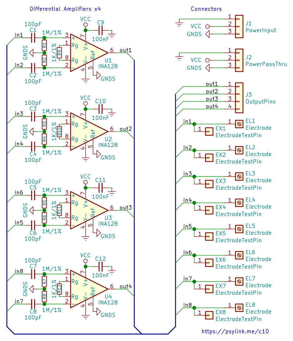
The front-side of the :
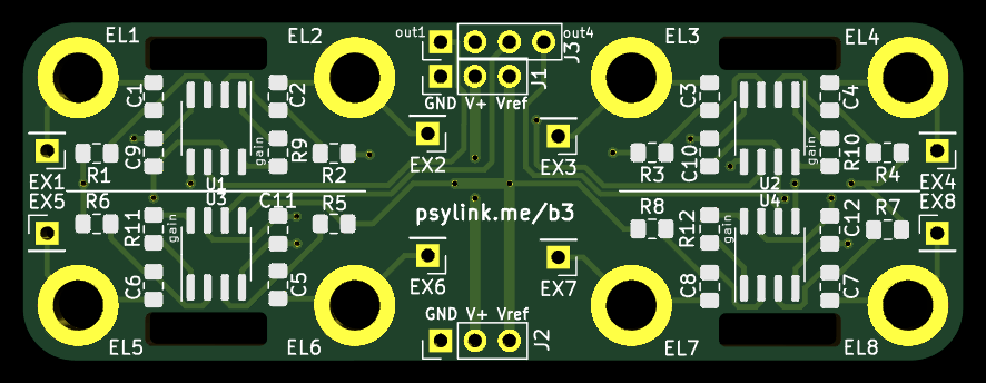
The four wide holes in the board are connection points for rubber bands, and the eight round metal-plated holes are mounting points the electrodes. These consist of a screw on one side, a nut on the other, holding both metal pieces tightly in place.
The electrodes can be spacer screws like these or dome nuts like these. While the spacer screws seem to pick up a better signal, the dome nuts are considerably more comfortable thanks to the rounded cap, so I think I'll stick with these for now.
Dome nuts are also called "hutmutter" in German, which translates to "hut's mother" (my nickname is hut), so just because of that fact, I had to try them out.
Additionally, one can use the pins EX1 through EX8 to connect arbitrary external electrodes.
A first prototype using and Power Module 3.1 (with an improvised rubber band mounting mechanism) can be seen here:

I played around with using off-the-shelf wet EMS (electric muscle stimulation) electrodes for the ground electrode, since good connectivity for the ground electrode is important for a good signal.
I did not find an improvement in the signal though, perhaps wet electrodes are not worth it.
Finally, the global microchip shortage has affected this project as well, and I could not find any sources for the power converter chips (TPS61220 DCKR) that boost the battery voltage of 1.2V to the required 5.0V. I still have some legit chips left, but in the long term, I need more of these, so I acquired some chips from Shenzhen via AliExpress. They have been advertised as "Original new, 100% quality", so what could POSSIBLY go wrong? But I tried them out, and they actually do their job quite nicely.
Future plans
The power module is currently only clumsily attached to the rubber band. The finished Prototype 8 will need a power module that's more compatible with the , by making it as long as the , and either by adding rubber band mounting holes, or by adding pin headers so that it can be stacked on top of the amplifier board, which would reduce the number of dangling wires as well.
I will also try out cheaper differential amplifiers to reduce the total cost of the device from ~70€ to ~30€ (excluding the ~39€ for the Arduino Nano 33 BLE Sense).
Neurofeedback: Training in both directions
└2021-07-17, by RomanFor now, the training of neural networks mostly happens on the AI side. The human makes arm gestures and presses keys on the keyboard. This provides the input (electrode and IMU signals) as well as the output/labels (keyboard actions) to the artificial neural network, which then learns the correlation between the two through supervised gradient descent.
Now I'm looking into how to train both the neural network of the AI as well as the nervous system of the user through neurofeedback, that is, by making the user more aware of their neural signals, which in turn allows them to fine-tune these.
My hope is that this will make up for the low quality of information that's available to the AI, due to noise, attenuation, and the low number/quality of electrodes. The user neither knows what signals the electrodes can access, nor how to willingly produce movements that create these signals. Some gestures work well, while others can't be detected at all, so the best bet is to use forceful gestures with maximal muscle activation. But if there was some sort of feedback to the user, like a visualization of the data that the neural network is extracting, the user could focus on the movements that work, and gradually lower the intensity, perhaps to the point where no actual movement is required anymore.
Of course there is already some feedback about the signals: The PsyLink UI shows the amplitude of each electrode in a rolling graph, and the GNURadio application shows detailed plots of the raw signals, both of which already help determining which movements will work for gestures and which will not. But the AI can of course combine, cross-correlate, filter, convolve and deconvolve the signals, which enables it to extract information that a human won't see in the raw signal data.
Ultimately, the goal is that the user learns to, on demand, fire off just enough neurons that PsyLink can pick up the signal and trigger the intended key press without any visible movement of the arm.
Approach
As described above, simply presenting the user with the raw electrode data is insufficient. A machine-learning approach will likely be optimal here, to overcome the preconceptions of a top-down designer. Since we already have an artificial neural network, why not use that one to generate the visualizations too?
In my current version of this idea:
- The user needs to invent some arbitrary gesture that should correspond to the action "Press key 'A'".
- The user is repeatedly asked to perform the gesture by the UI
- At random intervals
- For random durations
- With 2-3 seconds of heads-up warning to account for reaction time
- In between the gestures, the user should perform random other activities, but never do the gesture without being asked by the UI
- The AI is trained on the fly with
- Electrode signals as input
- A binary label of "Key 'A' pressed" vs. "Key 'A' not pressed" as output
- Each data point is added randomly (80:20) to the training or validation dataset
- After X seconds of collecting data, the AI is trained for Y epochs
- Every Z milliseconds, the AI is asked to predict the output from the current
input, and the neural activations of the last non-output layer of the NN
are presented to the user visually, along with the predicted output.
- The visualization could be a heatmap or a scatterplot, for example
- The visualization should cover a large dynamic range (both small changes and large changes to the values should be easily visible)
- Using the feedback, the user can tweak their gesture as desired, to e.g.
- Minimize the movement required to trigger the key
- Maximize the reliability with which the key press is predicted
- Over time, old data is dropped from the NN training to refine the visualization and to keep the training time short.
Once the user is ready, they can add a second action like "Press key 'B'" and so on.
New Frontpage + Logo
└2021-07-06, by RomanThe front page now looks a little more "modern", and I changed the logo from

to

Once again, this was inspired by the System Shock 2 Trioptimum logo.
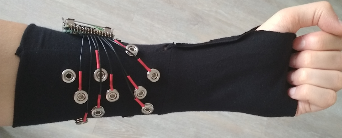
Cyber Wristband of Telepathy +2 [UNIQUE ITEM]
└2021-06-24, by Romanfinally found a home: Sleeve 4. Looks a bit like a Pip-Boy from the Fallout Series :)

Under the hood there's 9 electrodes (1x ground, 8x signal):